Soldering Workshop Assembly Guide
Introduction
The PCB
This PCB was designed with two levels of functionality. Depending upon your desired level of difficulty and time commitment, you can adjust the parts that populate your board. It is recommended to do level one and two on the same board if you want to solder both circuits; however, they do operate independently of one another.
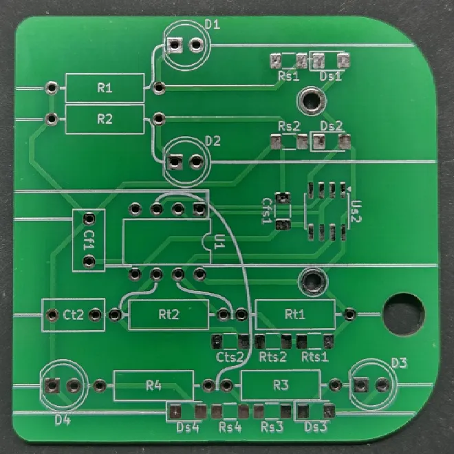
Collect Parts
Level 1 - Two Static LEDs
- 2x LED
- 2x Brightness Resistor (~300R)
- 1x Battery Connector
- 2x CR2016 Batteries
Level 2 - Two Blinking LEDs
- Selecting resistor/capacitor values roughly in line with this guide will result in a ~1Hz pulse between the LEDs with a pulse ratio that is close to 1:1. Use the 555 astable circuit calculator if you would like a different pulse rate and/or ratio.
- 2x LED
- 2x Brightness Resistor (~300R)
- 2x Timing Resistor (1x ~300R and 1x ~1M)
- 1x Timing Capacitor (1uF)
- 1x Power Filtering Capacitor (~50nF)
- 1x 555 Timing Chip
- 1x Battery Connector
- 2x CR2016 Batteries
Assembly
Level 1 Assembly
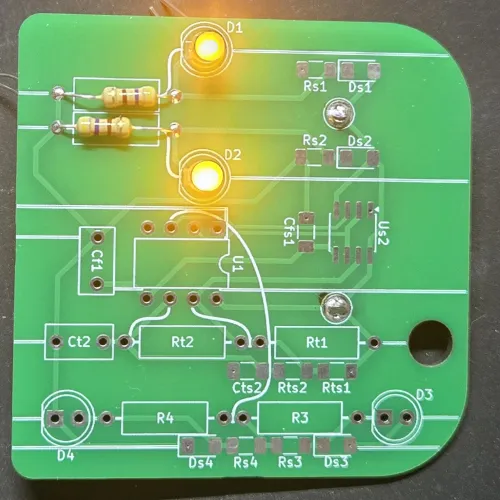
- Brightness Resistors in R1 and R2
- LEDs in D1 and D2
- Through-Hole: The shorter (negative) lead goes with the square pad or the flat side of the footprint.
- SMD: The green arrow points to the negative terminal which should go on the left pad.
- Battery Connector aligned with PCB footprint
Level 2 Assembly

- Brightness Resistors in R3 and R4
- LEDs in D3 and D4
- Timing Resistor 1 (<1k Ohm) in Rt1
- Timing Resistor 2 (>500k Ohm) in Rt2
- Power Filtering Capacitor in Cf1 (~50nF)
- Timing Capacitor in Ct2 (25-100nF)
- 555 Timer aligned with PCB footprint
- SMD 555 dot should be top left
- Battery Connector aligned with PCB footprint
Additional Circuit Information
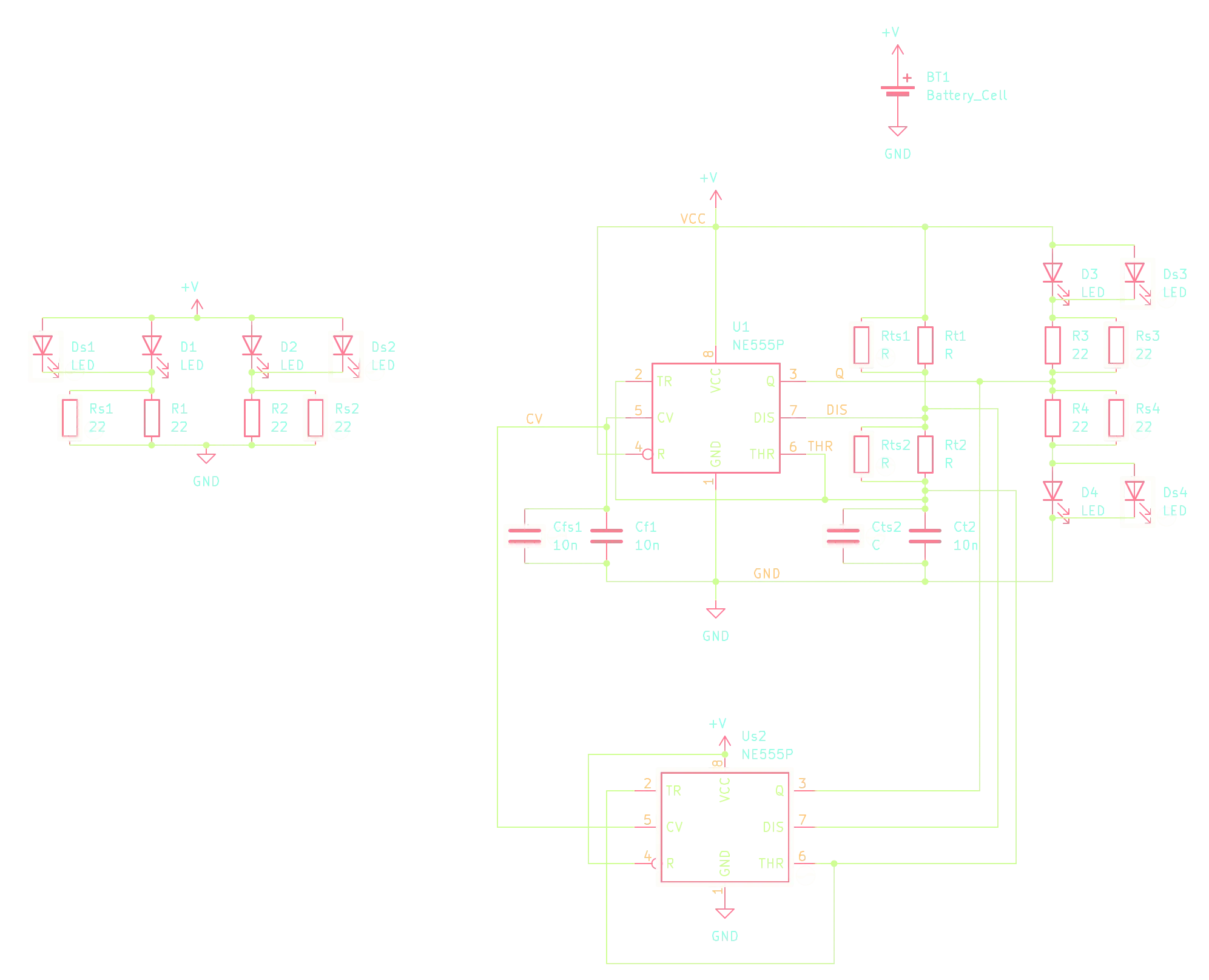
L1 Circuit
The level one circuit is fairly simple. The battery supplies power to the two static LEDs after passing through brightness limiting resistors. We are stacking CR2016s to run them in series resulting in a power supply of ~6V.
L2 Circuit
- NE555 Datasheet
- 555 astable circuit calculator The level two circuit is where things get interesting. Retaining our power supply of ~6V, we are now expecting to power the L1 circuit, two additional LEDs, and a 555 timer. According to the datasheet, it is recommended to supply a minimum of 4.5V to the 555. We have tested extensively with a single CR2032, and under most condidtions the circuit still functions. If the circuit contains power hungry blue or white LEDs, large timing resistors, or a very large timing capacitor, the circuit will typically cycle once and then not have enough juice to reset. It is generally understood that the output voltage of the 555 is ~2V lower than its input voltage. It stands to reason that the circuit would not cycle if the output voltage roughly equals the voltage required to power the receiving LED.
Our PCB uses the 555 in an astable configuration, which means the circuit will loop continuously until it is no longer receiving power. Generally speaking, the loop is as follows:
- Charging Phase (D4 On)
- Ct2 is completely empty
- Power flows from the battery to pin 8 on the 555
- Pin 3 of the 555 supplies power to R4/D4, Rt1/Rt2, and Ct2
- Ct2 begins charging
- Discharging Phase (D3 On)
- Once Ct2 reaches a voltage equal to 2/3 VCC, the 555 flips from charging Ct2 to discharging Ct2
- Incoming power is now sent to ground
- Power from the battery now has a path through R3/D3 to ground which lights up that LED
- Reset Phase
- Once Ct2 discharges enough power to output only 1/3 of VCC, the 555 flips again
- The 555 switches back to its initial state, sending power to R4/D4, Rt1/Rt2 and Ct2
Now that we have covered what is going on with R4/D4, we can take a look at R3/D3. If you look at the circuit diagram, you will notice that R3 and the negative terminal of D3 are connected to pin 3 of the 555 timer. You will also notice that VCC (power input) has a path to the positive terminal of D3. This means that when the 555 is supplying power to R4/D4 and the rest of the timing circuit, it is also supplying voltage roughly equal to VCC to D3 through R3. This results in a condition where voltage on either side of the diode is equal and electricity cannot flow through. Once power to R4/D4 is cut, voltage from VCC now through R3/D3 to Pin 3 of the 555 which is connected to ground.